- 您现在的位置:买卖IC网 > Sheet目录1234 > NCP5181BAL36WEVB (ON Semiconductor)BOARD EVAL NCP5181 36 W BALLAST
�� �
�
�NCP5181�
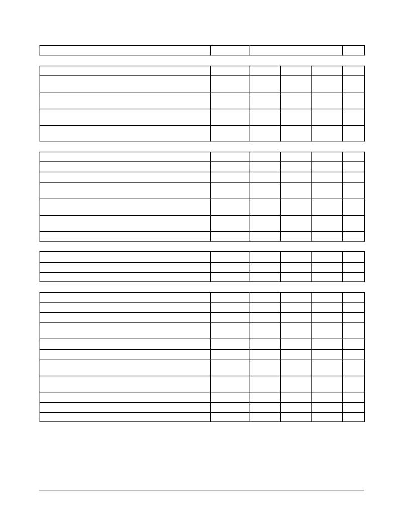
�ELECTRICAL� CHARACTERISTICS� (V� CC� =� V� boot� =� 15� V,� V� gnd� =� V� bridge� ,� ?� 40� °� C� <� T� A� <� 125� °� C,� Outputs� loaded� with� 1� nF)�
�Rating�
�Symbol�
�T� A� ?� 40� °� C� to� 125� °� C�
�Units�
�OUTPUT� SECTION�
�Min�
�Typ�
�Max�
�Output� High� Short� Circuit� pulsed� Current�
�V� DRV� =� 0� V,� PW� ≤� 10� m� s,� (Note� 1)�
�Output� Low� Short� Circuit� Pulsed� Current�
�V� DRV� =� V� CC� ,� PW� ≤� 10� m� s,� (Note� 1)�
�Output� Resistor� (Typical� Value� @� 25� °� C� Only)�
�Source�
�Output� Resistor� (Typical� Value� @� 25� °� C� Only)�
�Sink�
�I� DRVhigh�
�I� DRVlow�
�R� OH�
�R� OL�
�?�
�?�
�?�
�?�
�1.4�
�2.2�
�5�
�2�
�?�
�?�
�12�
�8�
�A�
�A�
�W�
�W�
�DYNAMIC� OUTPUT� SECTION�
�Rating�
�Turn� ?� on� Propagation� Delay� (V� bridge� =� 0� V)�
�Turn� ?� off� Propagation� Delay� (V� bridge� =� 0� V� or� 50� V)� (Note� 2)�
�Output� Voltage� Risetime�
�(from� 10%� to� 90%� @� V� CC� =� 15� V)� with� 1� nF� Load�
�Output� Voltage� Falling� Edge�
�(from� 90%� to� 10%� @� V� CC� =� 15� V)� with� 1� nF� Load�
�Propagation� Delay� Matching� between� the� High� Side� and� the� Low� Side�
�@� 25� °� C� (Note� 3)�
�Minimum� Input� Pulse� Width� that� Changes� the� Output�
�Symbol�
�t� ON�
�t� OFF�
�t� r�
�t� f�
�D� t�
�t� PW�
�Min�
�?�
�?�
�?�
�?�
�?�
�?�
�Typ�
�100�
�100�
�40�
�20�
�20�
�?�
�Max�
�170�
�170�
�60�
�40�
�35�
�100�
�Units�
�ns�
�ns�
�ns�
�ns�
�ns�
�ns�
�INPUT� SECTION�
�Low� Level� Input� Voltage� Threshold�
�Input� Pulldown� Resistor� (V� IN� <� 0.5� V)�
�High� Level� Input� Voltage� Threshold�
�V� IN�
�R� IN�
�V� IN�
�?�
�?�
�2.3�
�?�
�200�
�?�
�0.8�
�?�
�?�
�V�
�k� W�
�V�
�SUPPLY� SECTION�
�V� CC� UV� Startup� Voltage� Threshold�
�V� CC� UV� Shutdown� Voltage� Threshold�
�Hysteresis� on� V� CC�
�V� boot� Startup� Voltage� Threshold� Reference� to� Bridge� Pin�
�(V� boot_stup� =� V� boot� ?� V� bridge� )�
�V� boot� UV� Shutdown� Voltage� Threshold�
�Hysteresis� on� V� boot�
�Leakage� Current� on� High� Voltage� Pins� to� GND�
�(V� BOOT� =� V� BRIDGE� =� DRV_HI� =� 600� V)�
�Consumption� in� Active� Mode�
�(V� CC� =� V� boot� ,� f� sw� =� 100� kHz� and� 1� nF� Load� on� Both� Driver� Outputs)�
�Consumption� in� Inhibition� Mode� (V� CC� =� V� boot� )�
�V� CC� Current� Consumption� in� Inhibition� Mode�
�V� boot� Current� Consumption� in� Inhibition� Mode�
�V� CC_stup�
�V� CC_shtdwn�
�V� CC_hyst�
�V� boot_stup�
�V� boot_shtdwn�
�V� boot_shtdwn�
�I� HV_LEAK�
�I� CC1�
�I� CC2�
�I� CC3�
�I� CC4�
�7.9�
�7.3�
�0.3�
�7.9�
�7.3�
�0.3�
�?�
�?�
�?�
�?�
�?�
�8.9�
�8.2�
�0.7�
�8.9�
�8.2�
�0.7�
�0.5�
�4.5�
�250�
�215�
�35�
�9.8�
�9.0�
�?�
�9.8�
�9.0�
�?�
�40�
�6.5�
�400�
�?�
�?�
�V�
�V�
�V�
�V�
�V�
�V�
�m� A�
�mA�
�m� A�
�m� A�
�m� A�
�*Note:� see� also� characterization� curves�
�1.� Guaranteed� by� design.�
�2.� Turn� ?� off� propagation� delay� @� V� bridge� =� 600� V� is� guaranteed� by� design�
�3.� See� characterization� curve� for� D� t� parameters� variation� on� the� full� range� temperature.�
�4.� Timing� diagram� definition� see� Figures� 4,� 5� and� 6.�
�http://onsemi.com�
�4�
�发布紧急采购,3分钟左右您将得到回复。
相关PDF资料
NCV73810V2GEVB
BOARD EVAL FLEXRAY BUS NCV7381
NF20AA0509MHL
CURRENT LIMITER INRUSH 5OHM 20%
NHD-4.3-480272MF-20
BOARD CTRLR FOR NHDEV 4.3 TFT
NHDEV DEVELOPMENT BOARD
BOARD DEV LCD COG TFT 100X95MM
NP0120TAT1G
IC PROTECTOR LOW CAP 12V 5TSOP
NP1500SCT3G
THYRISTOR TSPD 100A 150V SMB
NP2600SCMCT3G
IC TSPD SURGE DEVICE 150MA SMB
NP3100SBMCT3G
IC TSPD SURGE PROTECT 80A SMB
相关代理商/技术参数
NCP5181DR2G
功能描述:功率驱动器IC HV MOSFET DRIVER RoHS:否 制造商:Micrel 产品:MOSFET Gate Drivers 类型:Low Cost High or Low Side MOSFET Driver 上升时间: 下降时间: 电源电压-最大:30 V 电源电压-最小:2.75 V 电源电流: 最大功率耗散: 最大工作温度:+ 85 C 安装风格:SMD/SMT 封装 / 箱体:SOIC-8 封装:Tube
NCP5181DR2G-CUT TAPE
制造商:ON 功能描述:NCP Series 2.2 A 20 V 2 Ohm SMT High Voltage High and Low Side Driver - SOIC-8
NCP5181PG
功能描述:功率驱动器IC HV MOSFET DRIVER RoHS:否 制造商:Micrel 产品:MOSFET Gate Drivers 类型:Low Cost High or Low Side MOSFET Driver 上升时间: 下降时间: 电源电压-最大:30 V 电源电压-最小:2.75 V 电源电流: 最大功率耗散: 最大工作温度:+ 85 C 安装风格:SMD/SMT 封装 / 箱体:SOIC-8 封装:Tube
NCP5201
制造商:ONSEMI 制造商全称:ON Semiconductor 功能描述:Dual Output DDR Power Controller
NCP5201/D
制造商:未知厂家 制造商全称:未知厂家 功能描述:Dual Output DDR Power Controller
NCP5201_06
制造商:ONSEMI 制造商全称:ON Semiconductor 功能描述:Dual Output DDR Power Controller
NCP5201MN
功能描述:DC/DC 开关控制器 DDR Dual Power RoHS:否 制造商:Texas Instruments 输入电压:6 V to 100 V 开关频率: 输出电压:1.215 V to 80 V 输出电流:3.5 A 输出端数量:1 最大工作温度:+ 125 C 安装风格: 封装 / 箱体:CPAK
NCP5201MNG
功能描述:DC/DC 开关控制器 DDR Dual Power RoHS:否 制造商:Texas Instruments 输入电压:6 V to 100 V 开关频率: 输出电压:1.215 V to 80 V 输出电流:3.5 A 输出端数量:1 最大工作温度:+ 125 C 安装风格: 封装 / 箱体:CPAK